[Photo Essay] An Intimate Look into Samsung’s Semiconductor Operations (Part 2)
Samsung Electronics was founded on the belief that the company’s most valuable asset is its people and that belief still stands true today. It’s not just capital expenditure or technology we invest in, but more importantly, in our people.
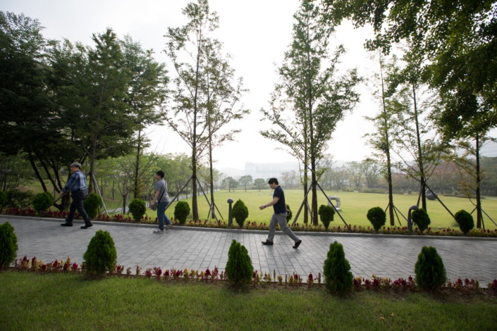
Coming to work may be a daily grind, but it helps if the walk to the office is a pleasant stroll. What also helps is that, under a few ground rules, employees use flexible working hours, making it easier to manage work-life balance.

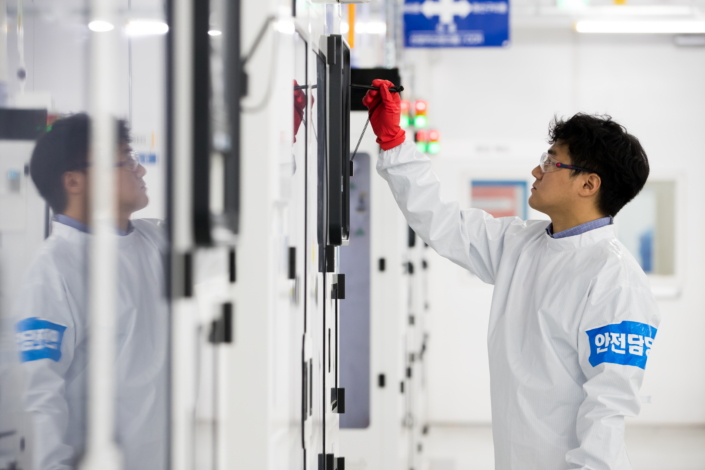
Semiconductors are fabricated in “cleanrooms,” where the environment is strictly managed to keep internal conditions, such as temperature, humidity and air pressure, at a constant level. Such measures are optimized for the ever-shrinking chips being manufactured, today mostly designed in nanometer (nm) scale, as well as for the workers inside.

Given the fact that 10nm is about one 10,000th the width of a single strand of hair, even a particle in few-cubic-micrometers could easily damage the circuits on our advanced chips. Workers wear “smocks” to prevent particles from being released into the cleanroom and would go through an air shower before entering the area. Even special paper and pens are required to take notes in there.
One of the key initiatives that go in tandem with efficient manufacturing is the safety of our workers on site. More than 500 safety professionals on staff oversee everyday operations and conduct regular inspections to ensure that all of our facilities comply with the most stringent regulations, locally and globally.
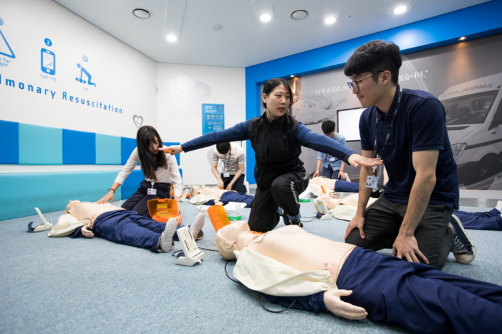
Every team within the company is required to train at least one of its members as an emergency care agent. The agents receive 16 hours of training on emergency response, including life-saving techniques such as CPR (cardiopulmonary resuscitation) and the Heimlich maneuver.
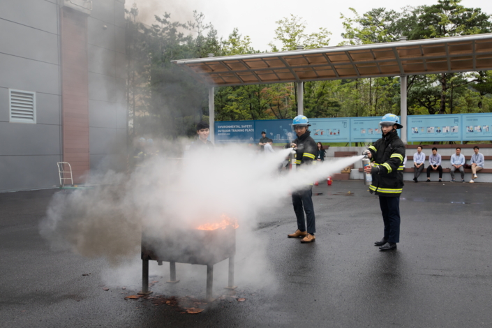
Employees are also trained to put out fires. As shown above, new hires begin safety training when they are initially hired and continue on a monthly basis throughout their careers based on a custom-curated curriculum.
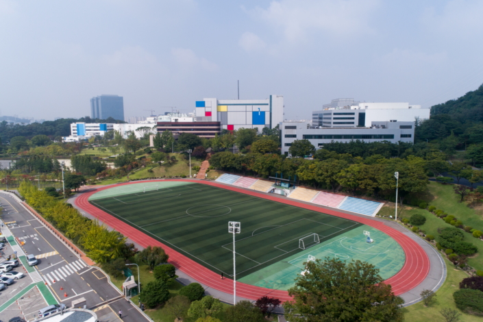
Of course, there is a lot of research, development and other day-to-day businesses that go on but it’s also vital for us to stay active. Several sports fields around campus as well as an indoor stadium are very popular with more than 160 inter-company sports clubs’ activities, company events and performances.

Even at tech companies, often the question of the day is what to have for lunch. Calories and sodium levels of each plate are displayed on the menu so that employees can make healthy and informed decisions about their diet.

The 12 cafeterias at the Giheung and Hwaseong campuses run 24-7, with up to 20 menu selections a day from all corners of the world that would tickle any palette.

A walk after lunch is an excellent way to start the afternoon. More than 600,000m2 of greenspace is managed in Giheung and Hwaseong campuses combined, an area equivalent to more than 75 soccer fields.

A coffee break under a tree is just as refreshing. More than 60,000 trees in Giheung and Hwaseong campuses include numerous species such as pine, oak, ginkgo and elm, which provide the perfect shade to cool off.

Employees can also look after their health by working out at one of the several gyms across campus that are equipped for weights, treadmill, swimming, pilates, squash and climbing. About 4,000 employees per day use the gyms regularly.

Personal trainers are also available on site to help you work out the muscles you didn’t know you had.

In case of the unfortunate event of feeling under the weather, employees can drop by the healthcare center on site for primary care from physicians, dentists, dermatologists, acupuncturists, pharmacists and counselors on staff. Physical therapy, musculoskeletal treatment and regular health checkup services are also available.
TAGSCMOSHwaseong CampusPhotoEssaySemiconductorSemiconductorSemiconductor industrySemiconductor OperationV-NAND technology
Corporate > People & Culture
Products > Semiconductors
Download
For any issues related to customer service, please go to
Customer Support page for assistance.
For media inquiries, please click Media Contact to move to the form.