Photostream (10,001/12,016) | Semiconductors
Eight Major Steps to Semiconductor Fabrication, Part 4: Drawing Structures in Nano-Scale
May 13, 2015
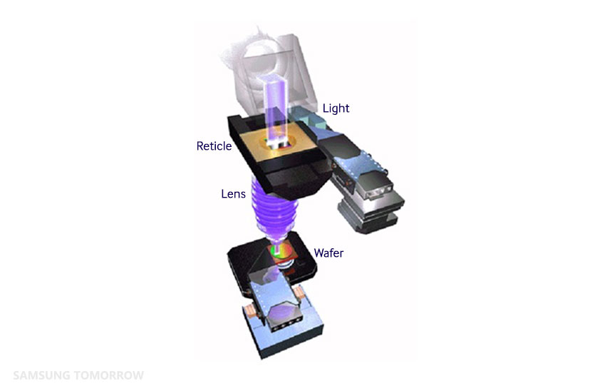
In the previous part of this series, our wafer got a protective layer of silicon oxide added to its surface. Now, let’s move on and find out about the photolithography process, through which electronic circuit patterns are transferred onto the wafer.
Before people began to take pictures with digital cameras or smartphones, there were analogue film cameras.
Drawing a circuit on a wafer via the photolithography—or ‘photo’ for short—process is quite similar to taking a picture and having a film developed. Let’s take a closer look.
For more information, please see :
https://news.samsung.com/global/eight-major-steps-to-semiconductor-fabrication-part-4-drawing-structures-in-nano-scale
