back
Semiconductors (762/819)
Eight Major Steps to Semiconductor Fabrication, Part 5: Etching a Circuit Pattern
May 20, 2015
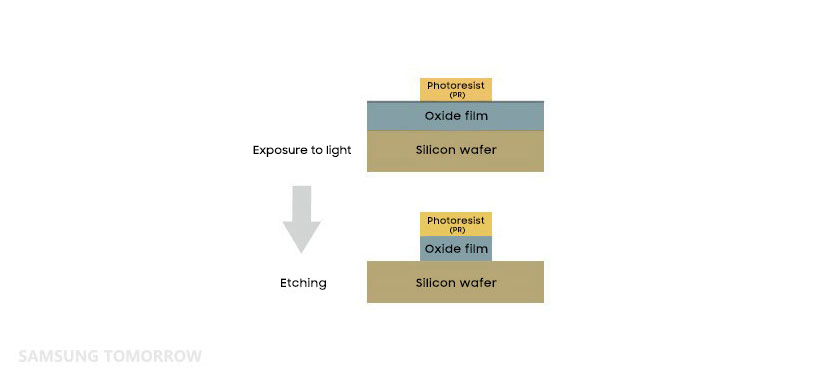
In the previous part of the series, we covered the photolithography, or “photo,” process in which circuit patterns were drawn on the wafer surface. Now, the wafer is ready go through the etching process to have any unnecessary materials removed so that only the desired patterns remain on its exterior.
For more information, please see :
https://news.samsung.com/global/eight-major-steps-to-semiconductor-fabrication-part-5-etching-a-circuit-pattern
