Eight Major Steps to Semiconductor Fabrication, Part 4: Drawing Structures in Nano-Scale
on May 13, 2015
In the previous part of this series, our wafer got a protective layer of silicon oxide added to its surface. Now, let’s move on and find out about the photolithography process, through which electronic circuit patterns are transferred onto the wafer.
Before people began to take pictures with digital cameras or smartphones, there were analogue film cameras.
Drawing a circuit on a wafer via the photolithography—or ‘photo’ for short—process is quite similar to taking a picture and having a film developed. Let’s take a closer look.
Designing circuits and creating a mask
The first step is to use computer-aided design (CAD) software and devise the circuits to be drawn onto the wafer. The size of this electronic circuit pattern can measure anywhere between 10 to 50 meters wide. This vast canvas bears a precisely designed, complex pattern that will end up on the semiconductor chips, which are about the size of a fingernail. Before this is carried out, an engineer actually steps onto the blown-up version of drawing to examine whether each part of the circuit is properly designed. The scale and the level of meticulousness required to accomplish this are quite amazing.

After examination, the pattern design is duplicated onto a glass substrate made of ultra-pure quartz with a beam of electrons, also known as an e-beam. A patterned substrate called a photoreticle, more commonly known as a photomask, which works like a negative film, is born.
Throughout the manufacturing process, the microscopic circuit has zero tolerance for any particles. As the patterned mask, which is larger than the actual chip size, passes through a reducer lens to transfer the design onto the chip, any particles that may be present on the mask could be shrunk as well. As such, particle contamination can be a significant problem during semiconductor manufacturing.
Picture-perfect technology
The photolithography process got its name from its role to transfer the circuit design onto a wafer by exposing the patterned mask to light. Making a replica on a wafer is like printing a black-and-white negative on light-sensitive paper.
Since the main focus of semiconductor technology is to scale the circuitry as small as possible, the first step to success is determined by the edge in photo process technologies. This is why continuous research in the photolithography field is a must to stay ahead.
Let’s take a closer look.
1. Making the wafer surface into a photographic print

First, photoresist (PR; highly sensitive to light) is applied evenly over the wafer surface. The additive can either be positive or negative depending on its reaction to light. Areas with positive photoresist are removed during the developing process when exposed to light, while those with negative photoresist remain. In other words, they create the image in the opposite way.
The PR layer needs to be thin, even and highly sensitive to ultraviolet rays to get the desired results.
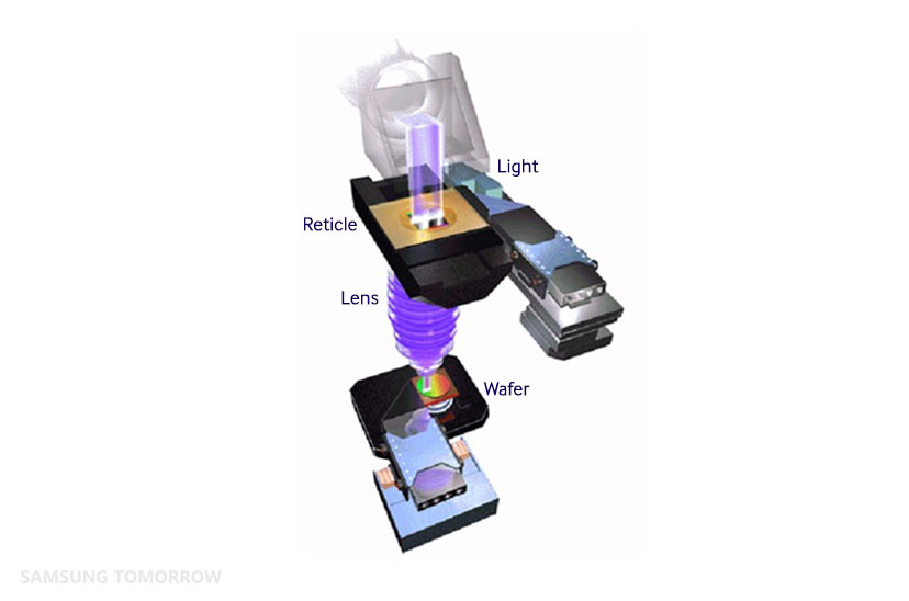
2. From film to print
The next steps are comparable to the process for developing photographs. After a wafer is prepared with the PR layer, it then goes through the stepper where the circuit design on the patterned mask is projected and transferred onto it with ultraviolet light. Due to the scale in semiconductor manufacturing, the area exposed to light is highly controlled and selective.
As developing solutions come in contact with the photoresist, certain areas are selectively removed to create the final pattern.
As such, our circuit designs are nicely traced onto the wafer.
Stay tuned for the next part of the series, where we will see how currents run through the microscopic circuits.
In Korean, http://samsungsemiconstory.tistory.com/136.