3D Technology has Taken Microchips into Another Dimension
on May 10, 2016
The ever-increasing demands of today’s electronic devices require smarter, faster semiconductors that use less energy. However, the advancements have been largely based on conventional chip designs, of which their two dimensional configurations are quickly approaching physical limits.
The industry’s solution to the dilemma was to adopt three dimensional concepts to semiconductor structures at several different stages of the engineering process, hence ‘3D semiconductor technologies.’
Here are some of the key ‘3D technologies’ that Samsung has introduced to the semiconductor industry, and how they tackled important technical challenges in meeting the market requirements.
14-nanometer FinFET

While conventional 2D transistors started to show several problems, including current leakage (a.k.a. short channel effect) that comes with finer technologies, the 14-nanometer (nm) FinFET technology raises a ‘fin’ that wraps over the conducting channel. This allows better control of the current in finer circuit designs. The new structure significantly decreases data leakage while demonstrating greater power advantages.
Samsung made this cutting-edge technology available at the end of 2014 which has enhanced hardware design and performance in today’s premium mobile devices.
Vertical NAND (V-NAND)
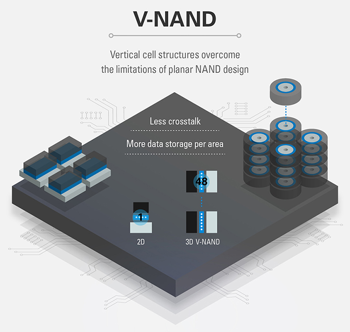
Advanced NAND flash technology at smaller design nodes started to experience issues with performance and durability, including data crosstalk.
In 2013, Samsung reached a breakthrough by mass producing V-NAND memory, which vertically stacks the cells with 3D Charge Trap Flash structures, which drastically increases density with less energy consumption and enhanced endurance. Samsung is currently mass producing its third-generation V-NAND lineup.
TSV (Through Silicon Via)
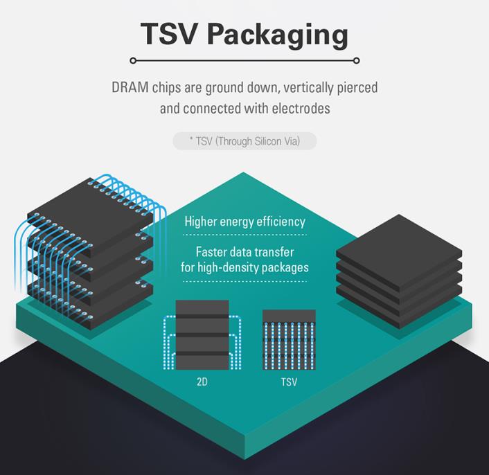
Instead of the traditional method of connecting the stacked dies externally with gold wire, we are now able to pierce hundreds of fine holes through the dies and then vertically connect them through the holes, allowing faster data processing with less power consumed. This technology is called 3D Through Silicon Via, or TSV.
Early this year, Samsung started mass producing the industry’s fastest DRAM package (4GB) based on the High Bandwidth Memory 2 (HBM2) interface. The state-of-the-art technology allows next-generation High Performance Computing systems and graphics cards brought to life.

For any issues related to customer service, please go to Customer Support pagefor assistance.
For media inquiries, please click Media Contactto move to the form.


