Eight Major Steps to Semiconductor Fabrication, Part 3: The Integrated Circuit
on May 6, 2015
In the previous part of this series, we explained how an oxide layer is formed and protects the wafer’s surface against impurities. Since the wafer is now protected with a silicon dioxide (SiO2) layer, it is ready to be imprinted with the circuit pattern, which contains the numerous densely packed electronic components such as transistors, diodes, resistors and capacitors. So, let’s take a look at how the designs for the microscopic structures are created.
Transistors herald a revolutionary change
Shortly before Christmas in 1947, a revolutionary discovery was made at the Bell Laboratories in New Jersey. William Shockley, John Bardeen and Walter Brattain learned that when a piece of semiconductor in lattice structure makes contact with conductive wires, electric signals are amplified. This finding led to a series of experiments, and the transistor, which was referred to as an amplifier in the early days, was born.
Transistors were first used in hearing aids and radios to amplify sound by boosting electric currents. They soon became a core element of many electronic goods. However, with time, electronics became more complex in their functions and so did their internal structures, resulting in a number of various setbacks.
A breakthrough occurred in 1958 when the complex electronic parts were put together in the form of a complex electronic circuit on a microscopic scale. These structures were named integrated circuits (IC).
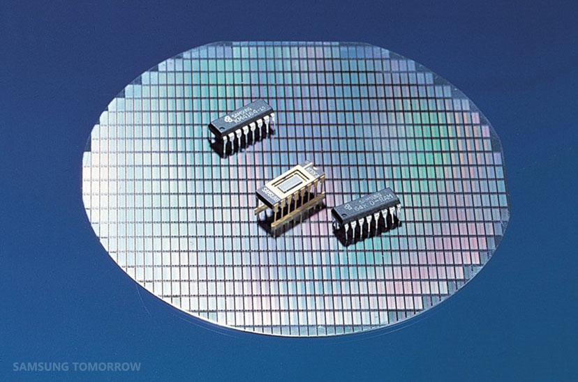
Integrated Circuits (IC)
Numerous transistors, diodes, resistors and capacitors are part of an integrated circuit, and are connected to each other seamlessly. These components respectively play different roles in processing and storing electric signals.
Transistors serve as a power switch, and capacitors store energy electrostatically in an electric field, just like a warehouse. Resistors control the current flow to other components while diodes manage the direction of that flow.
To fabricate an IC, a very minute and complex pattern on which all the circuitry are designed, is transferred onto multiple layers of materials. The transferring process utilizes photomasks that capture the miniaturized version of this pattern, just like film used for photographic printing.
If you’re curious about this photolithography process, we’ve got you covered; we’ll get to it in Part 4 of the series next week.
In Korean, http://www.samsungsemiconstory.com/133.