[Infographic] EUV, Samsung’s Latest Investment on Developing Next-generation Semiconductor Products
on October 18, 2018
Samsung Electronics is gaining recognition with its grand-scale investment in extreme ultraviolet (EUV) lithography technology. Recently Samsung started the production of the 7LPP, 7-nanometer (nm) LPP (Low Power Plus) with EUV, cementing its leadership in the industry and paving its way to produce an even thinner process node, down to the 3nm.
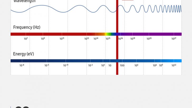
Semiconductors’ high performance and low power characteristics depend on the width of the circuits that are inserted into the chips’ limited space. In this sense, EUV realizes more detailed semiconductor circuit pattern than the existing argon fluoride (ArF) wavelength and reduces complex multi-patterning process, securing both high performance and productivity.
The EUV technology by Samsung is expected to accelerate the growth of various revolutionary products such as 5G, Artificial Intelligence and Internet of Things. Take a look at the infographic to learn more about EUV and how it is expected to contribute to the advancement of semiconductor technology.


