[Photo] Samsung Opens New State-of-the-Art Device Solutions Headquarters in Silicon Valley
USA on September 25, 2015

The building stands 170-feet high and has been designed to meet the LEED (Leadership in Energy and Environmental Design) standards of the U.S. Green Building Council.
More than 30 years of innovation and discoveries in Silicon Valley have helped define Samsung’s digital devices inside and out. On September 24, Samsung Electronics’ Device Solutions Division, part of its components business, celebrated the grand opening of its new American headquarters. Samsung’s DS teams have been spread across the area, and the brand new facility will join all team members together, allowing better communication across all disciplines.
Now home to R&D, marketing, sales and other teams, the new LEED-certified (Leadership in Energy and Environmental Design) 1.1 million-square-foot building will serve as a hub for state-of-the-art technologies in areas such as memory, logic, LED, displays and more.
Samsung is thrilled about the new facility. Let’s see how far it has come.

Employees can take a break in the peaceful courtyard located in the center of the building, one of the several open spaces around the facility.

The floor-to-ceiling windows create a bright space for employees to enjoy.

The open space design was chosen to encourage collaboration and enable frequent discussions.
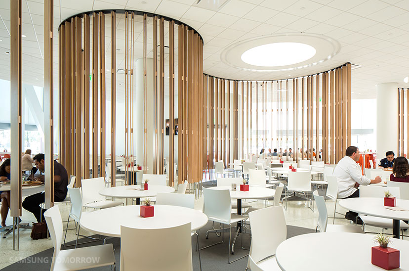
A modern food court is available all day for employees to visit.

The facility is composed of a series of two-story office “buildings” stacked on top of each other, each separated by “green floors” with gardens and recreational spaces that are part of an effort to re-introduce the natural environment in office architecture.

Samsung Semiconductor’s new North American headquarters in San Jose, CA is a ten-story building with approximately 1.1 million square feet of space.
Read more: