Samsung Starts Mass Producing Industry’s First 10-Nanometer Class DRAM
Korea on April 5, 2016

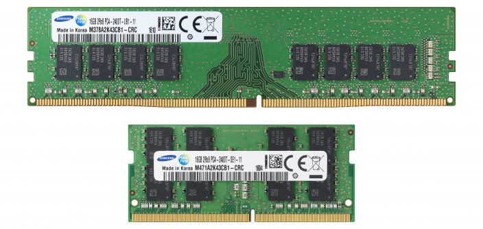
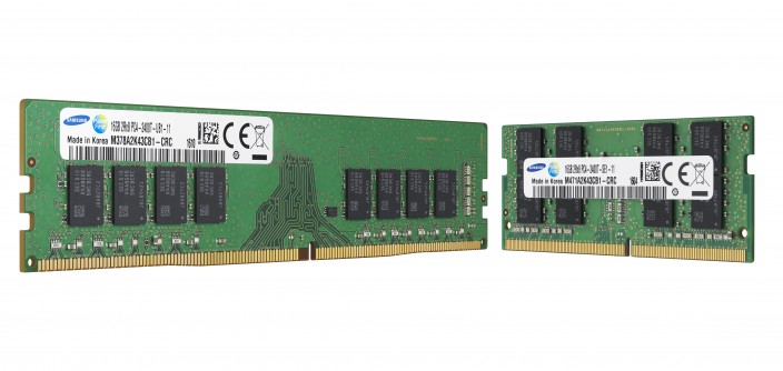
Samsung Electronics, the world leader in advanced memory technology, announced today that it has begun mass producing the industry’s first 10-nanometer (nm) class* , 8-gigabit (Gb) DDR4 (double-data-rate-4) DRAM chips and the modules derived from them. DDR4 is quickly becoming the most widely produced memory for personal computers and IT networks in the world, and Samsung’s latest advancement will help to accelerate the industry-wide shift to advanced DDR4 products.
Samsung opened the door to “10nm-class DRAM” for the first time in the industry after overcoming technical challenges in DRAM scaling. These challenges were mastered using currently available ArF (argon fluoride) immersion lithography, free from the use of EUV (extreme ultra violet) equipment.
Samsung’s roll-out of the 10nm-class (1x) DRAM marks yet another milestone for the company after it first mass produced 20-nanometer (nm)** 4Gb DDR3 DRAM in 2014.
“Samsung’s 10nm-class DRAM will enable the highest level of investment efficiency in IT systems, thereby becoming a new growth engine for the global memory industry,” said Young-Hyun Jun, President of Memory Business, Samsung Electronics. “In the near future, we will also launch next-generation, 10nm-class mobile DRAM products with high densities to help mobile manufacturers develop even more innovative products that add to the convenience of mobile device users.”
Samsung’s leading-edge 10nm-class 8Gb DDR4 DRAM significantly improves the wafer productivity of 20nm 8Gb DDR4 DRAM by more than 30 percent.
The new DRAM supports a data transfer rate of 3,200 megabits per second (Mbps), which is more than 30 percent faster than the 2,400Mbps rate of 20nm DDR4 DRAM. Also, new modules produced from the 10nm-class DRAM chips consume 10 to 20 percent less power, compared to their 20nm-process-based equivalents, which will improve the design efficiency of next-generation, high-performance computing (HPC) systems and other large enterprise networks, as well as being used for the PC and mainstream server markets.
The industry-first 10nm-class DRAM is the result of Samsung’s advanced memory design and manufacturing technology integration. To achieve an extremely high level of DRAM scalability, Samsung has taken its technological innovation one step further than what was used for 20nm DRAM. Key technology developments include improvements in proprietary cell design technology, QPT (quadruple patterning technology***) lithography, and ultra-thin dielectric layer**** deposition.
Unlike NAND flash memory, in which a single cell consists of only a transistor, each DRAM cell requires a capacitor and a transistor that are linked together, usually with the capacitor being placed on top of the area where the transistor rests. In the case of the new 10nm-class DRAM, another level of difficulty is added because they have to stack very narrow cylinder-shaped capacitors that store large electric charges, on top of a few dozen nanometer-wide transistors, creating more than eight billion cells.
Samsung successfully created the new 10nm-class cell structure by utilizing a proprietary circuit design technology and quadruple patterning lithography. Through quadruple patterning, which enables use of existing photolithography equipment, Samsung also built the core technological foundation for the development of the next-generation 10nm-class DRAM (1y).
In addition, the use of a refined dielectric layer deposition technology enabled further performance improvements in the new 10nm-class DRAM. Samsung engineers applied ultra-thin dielectric layers with unprecedented uniformity to a thickness of a mere single-digit angstrom (one 10 billionth of a meter) on cell capacitors, resulting in sufficient capacitance for higher cell performance.
Based on its advancements with the new 10nm-class DDR4 DRAM, Samsung expects to also introduce a 10nm-class mobile DRAM solution with high density and speed later this year, which will further solidify its leadership in the ultra-HD smartphone market.
While introducing a wide array of 10nm-class DDR4 modules with capacities ranging from 4GB for notebook PCs to 128GB for enterprise servers, Samsung will be extending its 20nm DRAM line-up with its new 10nm-class DRAM portfolio throughout the year.
*10nm-class denotes a process technology node somewhere between 10 and 19 nanometers, while 20nm-class means a process technology node somewhere between 20 and 29 nanometers.
**Samsung’s achievements in 2014 were about DDR3 and DDR4 products that used 20-nanometer process technology, which should be distinguished from 20nm-class process technology. The company’s first 20nm-class DRAM product actually came out three years earlier. In 2011, Samsung initiated production of 20nm-class 2Gb DDR3, and the year after, started producing a full line-up of DRAM product family that included 20nm-class 4Gb DDR3 and 4Gb LPDDR2 based packages and modules.
***Quadruple patterning is a multiple patterning technology that is used in high-end integrated circuit (IC) manufacturing, especially in the photolithography process. There are many different ways of deploying a multiple patterning technology, but the common goal is to extend the patterning resolution and enhance the feature density beyond that of conventional lithography.
****Dielectric materials are characterized by very low electrical conductivity in which an electric field can be sustained with minimal leakage. In semiconductor manufacturing, dielectric materials are used in many different steps. A major application of dielectric materials in Samsung’s 10nm-class DRAM manufacturing is to insulate capacitors and prevent electric leakage, which will result in a significant increase in capacitance and higher cell performance.
For any issues related to customer service, please go to Customer Support pagefor assistance.
For media inquiries, please click Media Contactto move to the form.