[Editorial] Making Semiconductor History: Contextualizing Samsung’s Latest Transistor Technology
on May 15, 2019
Documents, photographs and videos; audio files, spreadsheets and graphics; there are all kinds of complex forms of digital information stored in and transferred between the computers and smartphones in our everyday lives. However, the basis of how all digital information is expressed is in fact very simple; the binary numeral system, which only uses two symbols, ‘0’ and ‘1’.
A transistor is a semiconductor device used to transform the digital information coded in the binary system into electric signals. A transistor is composed of a ‘channel’ in which the electric current flows between the semiconductor’s source and its drain and a ‘gate’ for managing the electric current traveling through the channel. The gate generates binary system data by amplifying electric signals and also working as a switch. Because of this, the transistor is essentially the basic element of a semiconductor chip.

All digital information, be it in the form documents, photos or videos, is in fact a composed of the binary numeral system, which only uses two symbols, ‘0’ and ‘1’.
In order to increase the number of semiconductor chips mounted on the limited surface of a silicon (Si) substrate, the size of each semiconductor chip naturally needs to be decreased. Furthermore, in order to fit more new and complex functions into each semiconductor chip, the very basic element transistor must become smaller and its power consumption must be minimized to provide the longest possible battery lifespan, as well as reduced heat and electric charges. As electricity consumption is dependent on operating voltage, transistors have been developed so as to decrease operating voltage. Therefore, the history of the semiconductor is synonymous with the history of creating transistors that are smaller, faster and that consume less electricity.
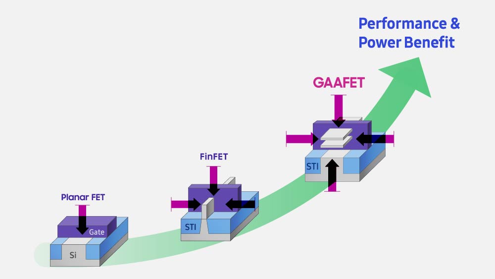
The history of the development of the semiconductor is synonymous with the history of creating transistors that are smaller, faster and that consume less electricity. From the left, Planar Transistor, Fully Depleted (Fin) Transistor, and GAA Transistor
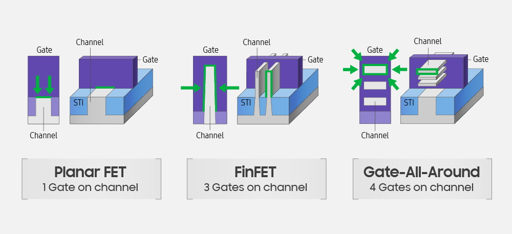
The most widely used transistor in the current semiconductor industry is the Metal-Oxide-Semiconductor (MOS). It consists of a metal electrode, an oxide insulator and a semiconductor channel. The first MOS transistor was of a planar architecture and was structured so that the gate and the channel made contact on one plane. But, as transistors become smaller, the distance between the source and the drain gets smaller, making it difficult for the gates to work as a switch. This is called a ‘short-channel effect’, and along with limiting voltage reduction, it means that planar transistors can only be applied to 20 or above nanometer nodes (or generations)1.
In order to overcome the short-channel effect, the Fully Depleted transistor emerged as the next generation of transistor. This transistor uses a thin silicon (Si) channel to avoid the short-channel effect by enhancing the ability of the gate to adjust the channel. Its structure format evolved out of that of the conventional transistor (a gate on a plane channel) to become a thin, rugged structure with a standing rectangular channel that interlocks with gates on three sides. As this thin, standing channel somewhat resembles a fish’s dorsal fin, it is also called the ‘fin transistor’. Samsung has been manufacturing fin transistors since 2012 in a range of sizes, starting at just 14 nanometers.
Whereas a planar transistor only allows the channel and the gate to contact in just one plane, a fin transistor has a 3-dimensional structure that allows three sides of a channel (excluding its bottom) to come into contact with the gates. This increased contact with the gates improves semiconductor performance as well as increasing the reduction of operating voltage, solving the problems brought about by the short-channel effect.
Nevertheless, the fin transistor is now facing limitations after several generations of developments and process transitions. Nowadays, the semiconductor industry is increasingly requiring transistors that can reduce operating voltage even further. Despite the fin transistor’s 3-dimensional structure, that only three of the four sides are in contact with gates is now becoming a limitation, as transistors themselves continue to progress and subsequently get smaller.
The evolution of semiconductor transistors
In order to mitigate the limitations of existing transistors solutions, Samsung has developed a new structure, the Gate-All-Around (GAA). As the name suggests, the GAA is a structure that maximizes gates’ channel-controlling function, as all channels, including the fourth bottom one, are covered by gates. The gates provide a 360-degree coverage of the entire channel area to eliminate the short-channel effect, resulting in reducing operating voltage further.
A typical GAA transistor takes the form of a thin and long nanowire2. However, a channel needs to be as wide as possible in order to allow a large amount of current to flow through it, and the small diameter of the nanowire makes obtaining this higher current flow difficult. To overcome this, Samsung created and patented their proprietary MBCFET™ (Multi-Bridge Channel Field Effect Transistor), an optimized version of the GAA transistor. The MBCFET™ increases the areas that make contact with gates by aligning wire-formed channel structures as a 2-dimensional nanosheets, which enables simpler device integration as well as increasing the electric current. Samsung’s MBCFET™ is a competitive transistor structure in that it not only includes the means to mitigate the short-channel effect thanks to the GAA structure, but it also increases performance by expanding the channel area.
Compared to existing 7-nanometer fin transistor process technology, the MBCFET™ decreases power consumption by 50%, improves performance by 30%, and reduces the area that the transistor takes up by 45%.

The development of GAA transistors, tantamount to the Industrial Revolution of semiconductor technology, is such a difficult process that Samsung is the only company currently offering a future delivery plan. Furthermore, the successful creation of the MBCFET™ is indicative of Samsung’s global industry-leading technological prowess. It has laid the foundation for transforming the semiconductor industry that was set to stall at the 4-nanometer scale, along with providing core technologies necessary for bringing about the fourth industrial revolution.
With this latest market-leading development, Samsung is paving the way for the future of the industry thanks to its collaborative approach and trailblazing technologies.
As a semiconductor engineer working in an industry that is entering an era of transformation brought about by new technology, I am very excited to see what the future holds.
1Nanometer is a measurement for a semiconductor. 1 nanometer is equal to one billionth of a meter.
2An ultra-tiny line that has one nanometer in section diameter
- Fin Transistor
- Fully Depleted Transistor
- GAA Transistor
- Gate-All-Around
- MBCFET™
- Multi-Bridge Channel Field Effect Transistor
- Nanosheet
- Nanowire
- Planar Transistor
- Samsung Semiconductors
- Semiconductors Leadership

For any issues related to customer service, please go to Customer Support pagefor assistance.
For media inquiries, please click Media Contactto move to the form.