[Editorial] 5nm: A Catalyst of the Fourth Industrial Revolution and What It Means for Semiconductor Innovations
on April 16, 2019
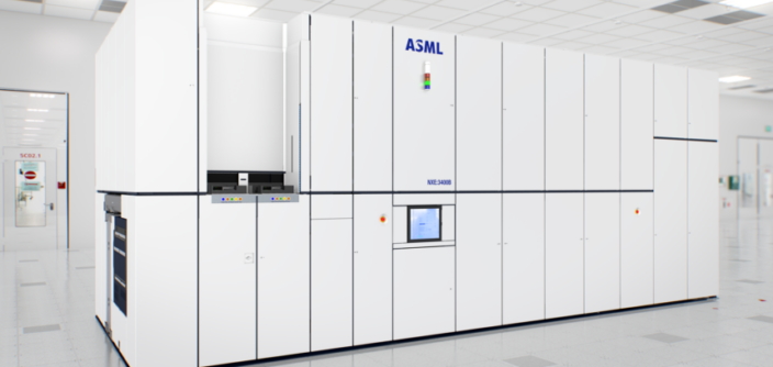
This week, Samsung Electronics announced that its 5-nanometer(nm) FinFET process technology based on EUV lithography is now ready for production. This is a remarkable accomplishment and testament to the capability of our colleagues at the S3 wafer fab in Hwaseong, Korea and their supply chain partners.
For me, what is most exciting about this milestone is that it highlights how far the semiconductor industry innovations have come today and provides a glimpse into the evolutions that will shape the industry of tomorrow.
Consider that the 5nm process is here in just six months after last October’s unveiling of the first commercial application of EUV in our 7nm process. It’s a rapid progress made possible in large part by running thousands of wafer layers through EUV exposure systems each week. Hands-on experience is the only way to ascend the EUV learning curve, and that body of knowledge is growing daily.
In the learning process, we’re seeing one of the biggest and broadest benefits of EUV – the simplification of design by moving away from increasingly complex multi-patterning lithography strategies. While still early, it’s increasingly clear that the reduced number of mask steps and more straightforward process is nothing short of a revolution for silicon designers. Sighs of relief will be heard as EUV will be seamlessly incorporated into the existing design architectures.
Samsung’s 5nm is the next step in the evolution of EUV. 5nm will be more efficient and feature new innovations including Samsung’s proprietary Smart Diffusion Break (SDB) transistor architecture. One of the most important aspects of 5nm is that it supports 25 percent area reduction and 10 percent performance improvement or 20 percent power reduction than 7nm.
Also, it will be largely design-rule compatible with the existing design of 7nm. Therefore, it is essentially a recharacterization of the technology, not redesign, which will substantially reduce time and the cost of implementation. This combination of technological advance and economic advantage is very much in line with a grand tradition of the semiconductor industry.
This merging of technological advancement and economic benefits is very much in line with the grand tradition in the semiconductor industry as well as technologies including 5G, AI, Connected & Automotive, Robot, etc. – constantly serving as a catalyst for the fourth industrial revolution, while simultaneously driving costs down. That’s why the evolution-moment of 5nm is, in its own unique way, as important as the innovation-moment of 7LPP.
Bringing EUV into production has been a long, challenging process. It required substantial investment of time, money, and human resources. While there were certainly moments of doubt along the way, we had to pursue our vision. The 5nm announcement offers compelling evidence for the value of the investment. As businesses from diverse fields including Foundry, Fabless, the Design House, Packaging, Tests, etc., the semiconductor ecosystem will grow stronger. This is a new chapter for the semiconductor industry, and we are excited to be part of the continued journey in innovation.
For any issues related to customer service, please go to Customer Support pagefor assistance.
For media inquiries, please click Media Contactto move to the form.