Samsung Successfully Completes 5nm EUV Development to Allow Greater Area Scaling and Ultra-low Power Benefits
Korea on April 16, 2019
Samsung Electronics makes major strides in EUV-based advanced nodes,
including 7nm mass production and 6nm customer tape-out
Samsung Electronics, a world leader in advanced semiconductor technology, today announced that its 5-nanometer (nm) FinFET process technology is complete in its development and now is ready for customers’ samples. By adding another cutting-edge node to its extreme ultraviolet (EUV)-based process offerings, Samsung is proving once again its leadership in the advanced foundry market.
Compared to 7nm, Samsung’s 5nm FinFET process technology provides up to a 25 percent increase in logic area efficiency with 20 percent lower power consumption or 10 percent higher performance as a result of process improvement to enable us to have more innovative standard cell architecture.
In addition to power performance area (PPA) improvements from 7nm to 5nm, customers can fully leverage Samsung’s highly sophisticated EUV technology. Like its predecessor, 5nm uses EUV lithography in metal layer patterning and reduces mask layers while providing better fidelity.
Another key benefit of 5nm is that we can reuse all the 7nm intellectual property (IP) to 5nm. Thereby 7nm customers’ transitioning to 5nm will greatly benefit from reduced migration costs, pre-verified design ecosystem, and consequently shorten their 5nm product development.
As a result of the close collaboration between Samsung Foundry and its ‘Samsung Advanced Foundry Ecosystem (SAFE™)’ partners, a robust design infrastructure for Samsung’s 5nm, including the process design kit (PDK), design methodologies (DM), electronic design automation (EDA) tools, and IP, has been provided since the fourth quarter of 2018. Besides, Samsung Foundry has already started offering 5nm Multi Project Wafer (MPW) service to customers.
“In successful completion of our 5nm development, we’ve proven our capabilities in EUV-based nodes,” said Charlie Bae, Executive Vice President of Foundry Business at Samsung Electronics. “In response to customers’ surging demand for advanced process technologies to differentiate their next-generation products, we continue our commitment to accelerating the volume production of EUV-based technologies.”
In October 2018, Samsung announced the readiness and its initial production of 7nm process, its first process node with EUV lithography technology. The company has provided commercial samples of the industry’s first EUV-based new products and has started mass production of 7nm process early this year.
Also, Samsung is collaborating with customers on 6nm, a customized EUV-based process node, and has already received the product tape-out of its first 6nm chip.
Mr. Bae continued, “Considering the various benefits including PPA and IP, Samsung’s EUV-based advanced nodes are expected to be in high demand for new and innovative applications such as 5G, artificial intelligence (AI), high performance computing (HPC), and automotive. Leveraging our robust technology competitiveness including our leadership in EUV lithography, Samsung will continue to deliver the most advanced technologies and solutions to customers.”
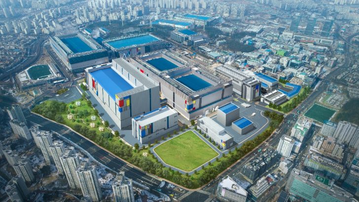
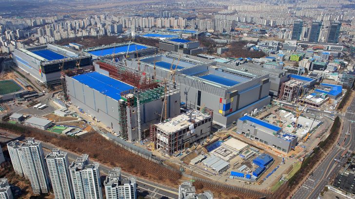
Samsung foundry’s EUV-based process technologies are currently being manufactured at the S3-line in Hwaseong, Korea. Additionally, Samsung will expand its EUV capacity to a new EUV line in Hwaseong, which is expected to be completed within the second half of 2019 and start production ramp-up from next year.