Samsung Begins Chip Production Using 3nm Process Technology With GAA Architecture
Korea on June 30, 2022
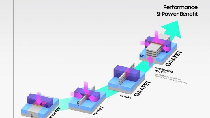
Optimized 3nm process achieves 45% reduced power usage, 23% improved performance and 16% smaller surface area compared to 5nm process

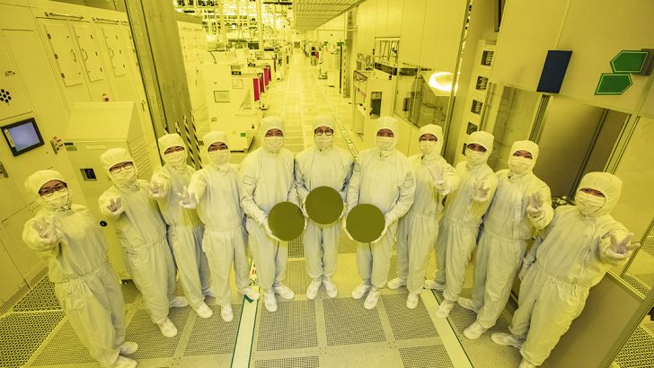
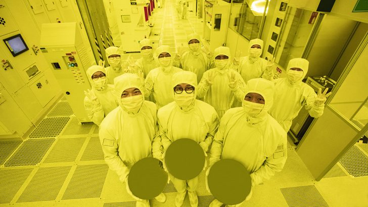
▲ The leaders of Samsung Foundry Business and Semiconductor R&D Center are holding up three fingers as a symbol of 3nm celebrating the company’s first ever production of 3nm process with GAA architecture.
Samsung Electronics, the world leader in semiconductor technology, today announced that it has started initial production of its 3-nanometer (nm) process node applying Gate-All-Around (GAA) transistor architecture.
Multi-Bridge-Channel FET (MBCFET™), Samsung’s GAA technology implemented for the first time ever, defies the performance limitations of FinFET, improving power efficiency by reducing the supply voltage level, while also enhancing performance by increasing drive current capability.
Samsung is starting the first application of the nanosheet transistor with semiconductor chips for high performance, low power computing application and plans to expand to mobile processors.
“Samsung has grown rapidly as we continue to demonstrate leadership in applying next-generation technologies to manufacturing, such as foundry industry’s first High-K Metal Gate, FinFET, as well as EUV. We seek to continue this leadership with the world’s first 3nm process with the MBCFET™,” said Dr. Siyoung Choi, President and Head of Foundry Business at Samsung Electronics. “We will continue active innovation in competitive technology development and build processes that help expedite achieving maturity of technology.”

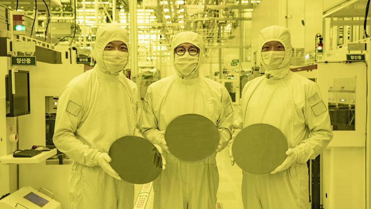
▲ (From left) Michael Jeong, Corporate Vice President; Ja-Hum Ku, Corporate Executive Vice President; and Sang Bom Kang, Corporate Vice President at Samsung Foundry Business are holding up 3nm wafers at the production line of Samsung Electronics Hwaseong Campus.
Design-Technology Optimization for Maximized PPA
Samsung’s proprietary technology utilizes nanosheets with wider channels, which allow higher performance and greater energy efficiency compared to GAA technologies using nanowires with narrower channels. Utilizing the 3nm GAA technology, Samsung will be able to adjust the channel width of the nanosheet in order to optimize power usage and performance to meet various customer needs.
In addition, the design flexibility of GAA is highly advantageous for Design Technology Co-Optimization (DTCO),1 which helps boost Power, Performance, Area (PPA) benefits. Compared to 5nm process, the first-generation 3nm process can reduce power consumption by up to 45%, improve performance by 23% and reduce area by 16% compared to 5nm, while the second-generation 3nm process is to reduce power consumption by up to 50%, improve performance by 30% and reduce area by 35%.

Providing 3nm Design Infrastructure & Services With SAFE™ Partners
As technology nodes get smaller and chip performance needs grow greater, IC designers face challenges of handling tremendous amounts of data to verify complex products with more functions and tighter scaling. To meet such demands, Samsung strives to provide a more stable design environment to help reduce the time required for design, verification and sign-off process, while also boosting product reliability.
Since the third quarter of 2021, Samsung Electronics has been providing proven design infrastructure through extensive preparation with Samsung Advanced Foundry Ecosystem (SAFE™) partners including Ansys, Cadence, Siemens and Synopsys, to help customers perfect their product in a reduced period of time.
Quotes from SAFE™ Partners
- Ansys, [John Lee, Vice President and General Manager of the Electronics, Semiconductor & Optics Business Unit at Ansys]
“Together, Ansys and Samsung continue to deliver enabling technology for the most advanced designs, now at 3nm with GAA technology. The signoff fidelity of our Ansys multiphysics simulation platform is testament to our continued partnership with Samsung Foundry at the leading edge. Ansys remains committed to delivering the best design experience for our mutual advanced customers.”
- Cadence, [Tom Beckley, Senior Vice President and General Manager, Custom IC & PCB Group at Cadence]
“We congratulate Samsung on this 3nm GAA production release milestone. Cadence worked closely with Samsung Foundry to enable customers to achieve optimal power, performance and area for this node using our digital solutions from library characterization to full digital flow implementation and signoff, all driven by our Cadence Cerebrus AI-based technology to maximize productivity. With our custom solutions, we collaborated with Samsung to enable and validate a full AMS flow to enhance productivity from circuit design and simulation through automated layout. We look forward to continuing this collaboration to achieve more tapeout successes.”
- Siemens EDA, [Joe Sawicki, Executive Vice President for the IC-EDA segment of Siemens Digital Industries Software]
“Siemens EDA is pleased to have collaborated with Samsung to help ensure that our existing software platforms also work on Samsung’s new 3-nanometer process node since the initial development phase. Our longtime partnership with Samsung through the SAFE™ program generates significant value for our mutual customers, by certification of Siemens industry-leading EDA tools at 3nm.”
- Synopsys, [Shankar Krishnamoorthy, General Manager and Corporate Staff for the Silicon Realization Group at Synopsys]
“Through our long-standing, strategic collaboration with Samsung Foundry, we are enabling our solutions to support Samsung’s advanced processes, helping our mutual customers significantly accelerate their design cycles. Our support for Samsung’s 3nm process with GAA architecture continues expanding, now with our Synopsys Digital Design, Analog Design and IP products, enabling customers to deliver differentiated SoCs for key high-performance computing applications.”
1 For more information on Design Technology Co-Optimization (DTCO), please see below links:
- 3nm Gate-All-Around
- FinFET
- Gate-All-Around
- High-K Metal Gate Process Technology
- Multi-Bridge Channel Field Effect Transistor
- Samsung Advanced Foundry Ecosystem
For any issues related to customer service, please go to Customer Support pagefor assistance.
For media inquiries, please click Media Contactto move to the form.