Samsung Introduces Far-reaching V-NAND Memory Solutions to Tackle Data Processing and Storage Challenges
USA on August 9, 2017

Samsung Electronics, the world leader in advanced memory technology, has announced new V-NAND (Vertical NAND) memory solutions and technology that will address the pressing requirements of next-generation data processing and storage systems. With the rapid increase of data-intensive applications across many industries using artificial intelligence and Internet of Things (IoT) technologies, the role of flash memory has become extremely critical in accelerating the speed at which information can be extracted for real-time analysis.
At the inaugural Samsung Tech Day* and this year’s Flash Memory Summit**, Samsung is showcasing solutions to address next-generation data processing challenges centered around the company’s latest V-NAND technology and an array of solid state drives (SSDs). These solutions will be at the forefront of enabling today’s most data-intensive tasks such as high-performance computing, machine learning, real-time analytics and parallel computing.
“Our new, highly advanced V-NAND technologies will offer smarter solutions for greater value by providing high data processing speeds, increased system scalability and ultra-low latency for today’s most demanding cloud-based applications,” said Gyoyoung Jin, executive vice president and head of Memory Business at Samsung Electronics. “We will continue to pioneer flash innovation by leveraging our expertise in advanced 3D-NAND memory technology to significantly enhance the way in which information-rich data is processed.
Samsung Heralds Era of 1-Terabit (Tb) V-NAND Chip
Samsung announced a 1Tb V-NAND chip that it expects to be available next year. Initially mentioned in 2013, during unveiling of the industry’s first 3D NAND, Samsung has been working to enable its core memory technologies to realize one terabit of capacity on a single chip using a V-NAND structure.
The arrival of a 1Tb V-NAND chip next year will enable 2TB of memory in a single V-NAND package by stacking 16 1Tb dies and will represent one of the most important memory advances of the past decade.
NGSFF (Next Generation Small Form Factor) SSD to Improve Server Storage Capacity and IOPS
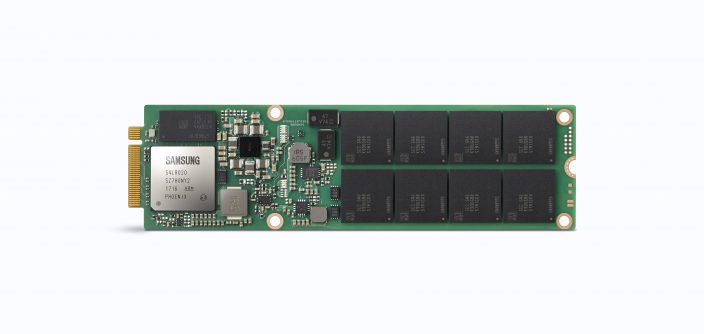
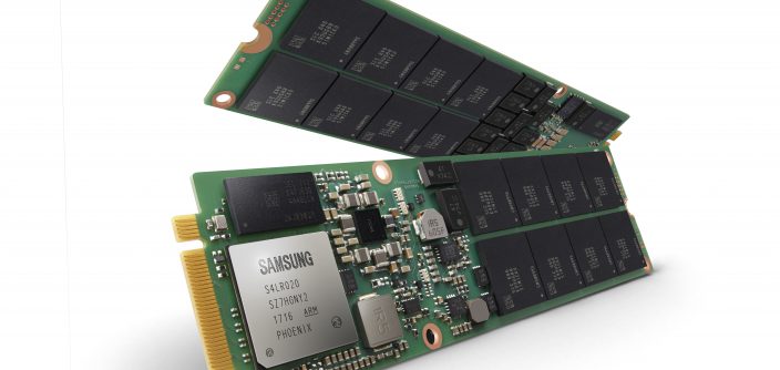
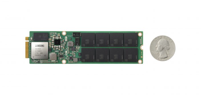
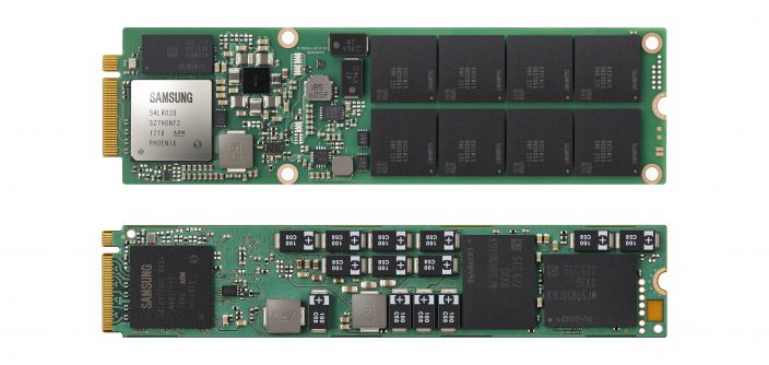
Samsung is sampling the industry’s first 16-terabyte (TB) NGSFF SSD, which will dramatically improve the memory storage capacity and IOPS (input/output operations per second) of today’s 1U rack servers. Measuring 30.5mm x 110mm x 4.38mm, the Samsung NGSFF SSD provides hyper-scale data center servers with substantially improved space utilization and scaling options.
Utilizing the new NGSFF drive instead of M.2 drives in a 1U server can increase the storage capacity of the system by four times. To highlight the advantages, Samsung demonstrated a reference server system that delivers 576TB in a 1U rack, using 36 16TB NGSFF SSDs. The 1U reference system can process about 10 million random read IOPS, which triples the IOPS performance of a 1U server equipped with 2.5-inch SSDs. A petabyte capacity can be achieved using only two of the 576TB systems.
Samsung plans to begin mass producing its first NGSFF SSDs in the fourth quarter of this year, while working to standardize the form factor with industry partners.
Z-SSD: Optimized for Systems Requiring Fast Memory Responsiveness
Following last year’s introduction of its Z-SSD technology, Samsung introduced its first Z-SSD product, the SZ985. Featuring ultra-low latency and high performance, the Z-SSD will be used in data centers and enterprise systems dealing with extremely large, data-intensive tasks such as real-time “big data” analytics and high-performance server caching. Samsung is collaborating with several of its customers on integrating the Z-SSD in upcoming applications.
The Samsung SZ985 requires only 15 microseconds of read latency time which is approximately a seventh of the read latency of an NVMe*** SSD. At the application level, the use of Samsung’s Z-SSDs can reduce system response time by up to 12 times, compared to using NVMe SSDs.
With its fast response time, the new Z-SSD will play a pivotal role in eliminating storage bottlenecks in the enterprise and in improving the total cost of ownership (TCO).
New Approach to Storage with Proprietary Key Value SSD Technology
Samsung also introduced a completely new technology called Key Value SSD. The name refers to a highly innovative method of processing complex data sets. With the sharply increasing use of social media services and IoT applications, which contribute to the creation of object data such as text, image, audio and video files, the complexity in processing this data increases substantially.
Today, SSDs convert object data of widely ranging sizes into data fragments of a specific size called “blocks.” The use of these blocks requires implementation processes consisting of LBA (logical block addressing) and PBA (physical block addressing) steps. However, Samsung’s new Key Value SSD technology allows SSDs to process data without converting it into blocks. Samsung’s Key Value instead assigns a ‘key’ or specific location to each ”value,” or piece of object data – regardless of its size. The key enables direct addressing of a data location, which in turn enables the storage to be scaled. Samsung’s Key Value technology enables SSDs to scale-up (vertically) and scale-out (horizontally) in performance and capacity. As a result, when data is read or written, a Key Value SSD can reduce redundant steps, which leads to faster data inputs and outputs, as well as increasing TCO and significantly extending the life of an SSD.
* Editor’s Note: Samsung Tech Day hosted at Samsung’s Silicon Valley headquarters on Monday August 7th, showcased “Samsung@the Heart of Storage” and provided insights into the company’s plans to deliver IT products that support the big data explosion, give greater access to massive real-time data sets, and provide real-time, fast data capabilities. The event also hosted an executive, customer and analyst panel, and displayed product demos across Samsung’s comprehensive product ecosystem.
** Editor’s Note: Flash Memory Summit (FMS), produced by Conference ConCepts, showcases the mainstream applications, key technologies and leading vendors that are driving the multi-billion dollar non-volatile memory and SSD markets. FMS is reportedly the world’s largest event featuring the trends, innovations, and influencers driving the adoption of flash memory in demanding enterprise storage applications, as well as in smartphones, tablets, and mobile and embedded systems. For more information, please visit at www.flashmemorysummit.com/
*** Editors’ Note: Often shortened as NVMe, NVM Express (Non-Volatile Memory Express) is a high performance, scalable host controller interface with a streamlined ‘register and command’ set that has been optimized for enterprise and client systems using PCIe SSDs. For more information, please visit www.nvmexpress.org

