Samsung Electronics Begins Mass Production at New Semiconductor Plant in Pyeongtaek, South Korea
Korea on July 4, 2017

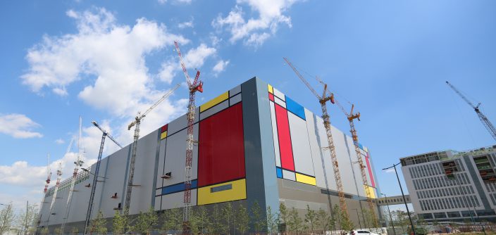
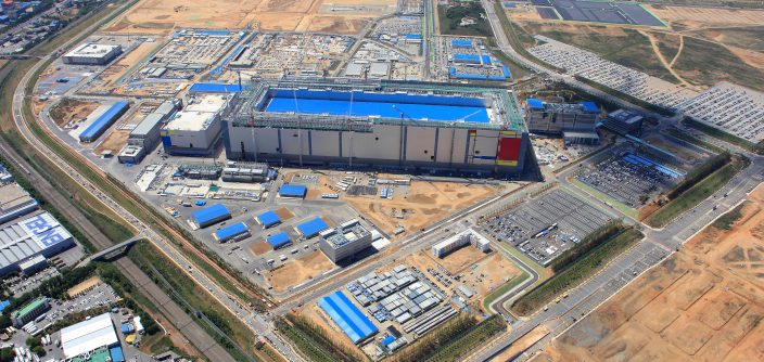
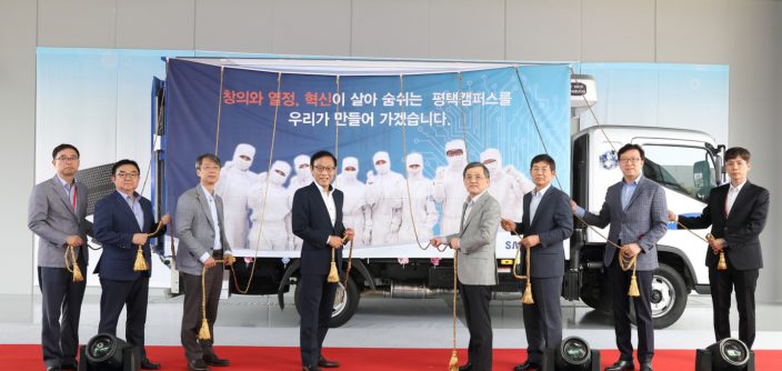
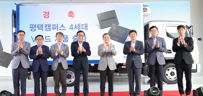
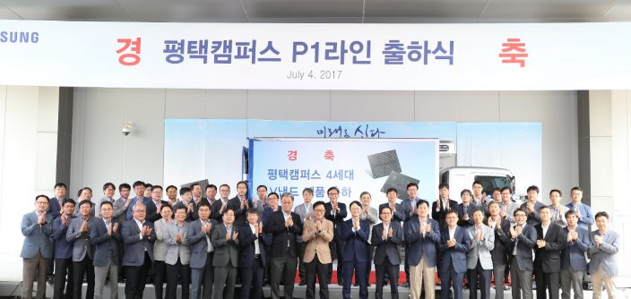
Samsung Electronics Pyeongtaek Line 1
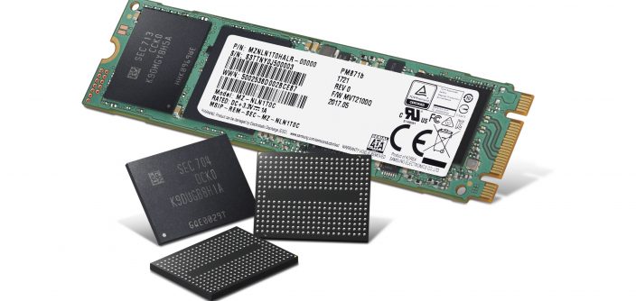
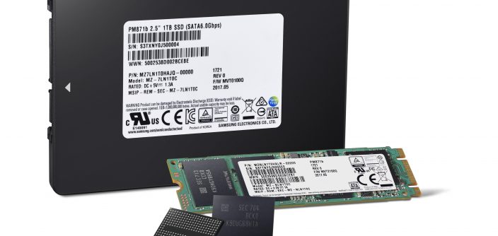
Samsung Electronics, a world leader in advanced semiconductor technology, today announced that its new semiconductor fabrication line in Pyeongtaek, South Korea, has begun mass production and shipping its first product to customers. The new facility will focus on the production of Samsung’s fourth-generation V-NAND (64 layers), adding to the company’s leading capacity for cutting-edge memory products.
“With the dedication and support of our employees, customers and partners, our new Pyeongtaek campus represents a new chapter in Samsung’s semiconductor operations,” said Oh-Hyun Kwon, Vice Chairman and Chief Executive Officer of Samsung Electronics.
With two years of construction since it broke ground in May, 2015, the fabrication line at the Pyeongtaek campus is currently the largest single Fab in the industry.
Recent emerging IT trends such as the Internet of Things (IoT), artificial intelligence (AI), big data and automotive technologies has sharply increased demand for next-generation components. In response to these market needs, Samsung, across both Samsung Electronics and Samsung Display, plans to reinforce its manufacturing capabilities by investing more than KRW 37 trillion in investments to its global production facilities.
- By 2021, Samsung will invest a total of KRW 30 trillion into its current Pyeongtaek line to expand its semiconductor fabrication capacity
- Samsung also plans to invest KRW 6 trillion in its Hwaseong, South Korea, site for a semiconductor fabrication line optimized to install state-of-the-art infrastructure including Extreme Ultra Violet (EUV) equipment
- Samsung Display is reviewing plans to establish a new OLED manufacturing site in Asan, South Korea, by 2018

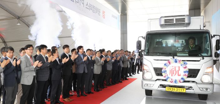
Samsung Electronics celebrated the first chip shipment from its new Pyeongtaek Line
In addition, Samsung’s plans to construct a second semiconductor fabrication line in Xi’an, China, site are also under review. Samsung’s first semiconductor fabrication line in Xi’an was constructed in 2014 and is presently in full operation.
With the new investments, Samsung aims to strengthen its global fabrication network and accelerate the overall development of the IT industry.
For any issues related to customer service, please go to Customer Support pagefor assistance.
For media inquiries, please click Media Contactto move to the form.