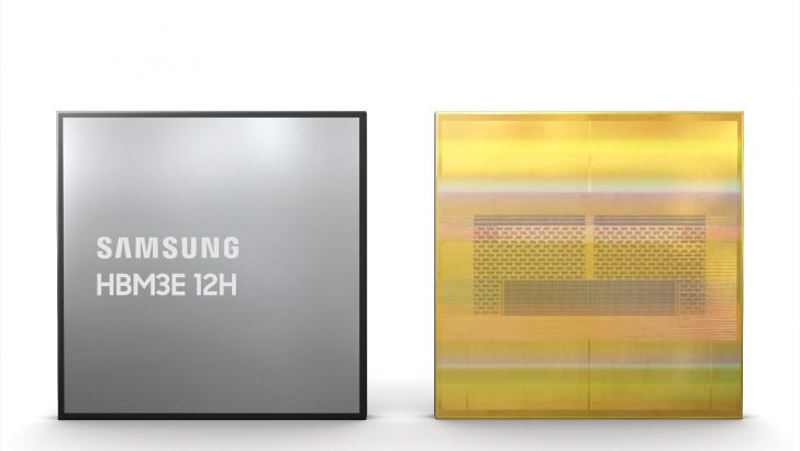
Samsung Develops Industry-First 36GB HBM3E 12H DRAM
Korea on February 27, 2024
Samsung’s HBM3E 12H achieves industry’s largest capacity HBM with groundbreaking 12-layer stack, raising both performance and capacity by more than 50%
Advanced TC NCF technology enhances vertical density and thermal properties
Samsung positioned to meet demand for high-performance and high-capacity solutions in the AI era

Samsung Electronics, a world leader in advanced memory technology, today announced that it has developed HBM3E 12H, the industry’s first 12-stack HBM3E DRAM and the highest-capacity HBM product to date.
Samsung’s HBM3E 12H provides an all-time high bandwidth of up to 1,280 gigabytes per second (GB/s) and an industry-leading capacity of 36 gigabytes (GB). In comparison to the 8-stack HBM3 8H, both aspects have improved by more than 50%.
“The industry’s AI service providers are increasingly requiring HBM with higher capacity, and our new HBM3E 12H product has been designed to answer that need,” said Yongcheol Bae, Executive Vice President of Memory Product Planning at Samsung Electronics. “This new memory solution forms part of our drive toward developing core technologies for high-stack HBM and providing technological leadership for the high-capacity HBM market in the AI era.”
The HBM3E 12H applies advanced thermal compression non-conductive film (TC NCF), allowing the 12-layer products to have the same height specification as 8-layer ones to meet current HBM package requirements. The technology is anticipated to have added benefits especially with higher stacks as the industry seeks to mitigate chip die warping that come with thinner die. Samsung has continued to lower the thickness of its NCF material and achieved the industry’s smallest gap between chips at seven micrometers (µm), while also eliminating voids between layers. These efforts result in enhanced vertical density by over 20% compared to its HBM3 8H product.
Samsung’s advanced TC NCF also improves thermal properties of the HBM by enabling the use of bumps in various sizes between the chips. During the chip bonding process, smaller bumps are used in areas for signaling and larger ones are placed in spots that require heat dissipation. This method also helps with higher product yield.
As AI applications grow exponentially, the HBM3E 12H is expected to be an optimal solution for future systems that require more memory. Its higher performance and capacity will especially allow customers to manage their resources more flexibly and reduce total cost of ownership (TCO) for datacenters. When used in AI applications, it is estimated that, in comparison to adopting HBM3 8H, the average speed for AI training can be increased by 34% while the number of simultaneous users of inference services can be expanded more than 11.5 times.1
Samsung has begun sampling its HBM3E 12H to customers and mass production is slated for the first half of this year.
1 Based on internal simulation results


