Samsung Electronics Brings Next Wave of High-Performance Storage with Mass Production of Fifth-generation V-NAND
Korea on July 10, 2018
Samsung’s new 256Gb V-NAND features industry’s fastest data transfer speed, while being the first to apply the ‘Toggle DDR 4.0’ NAND interface

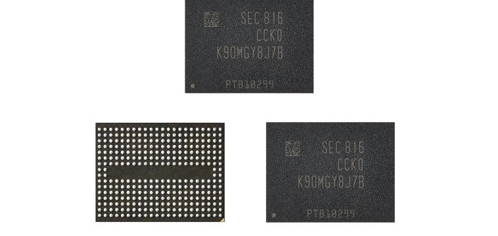
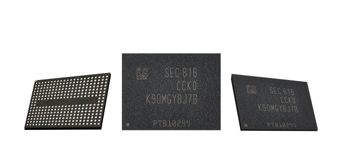
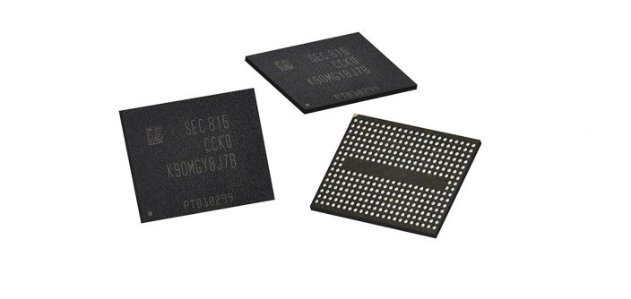
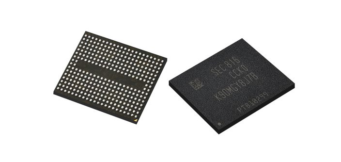
Samsung Electronics, the world leader in advanced memory technology, today announced that it has begun mass producing its fifth-generation V-NAND memory chips with the fastest data transfers now available. In the industry’s first use of the ‘Toggle DDR 4.0’ interface, the speed for transmitting data between storage and memory over Samsung’s new 256-gigabit (Gb) V-NAND has reached 1.4-gigabits per second (Gbps), a 40-percent increase from its 64-layer predecessor.
The energy efficiency of Samsung’s new V-NAND remains comparable to that of the 64-layer chip, primarily because the operating voltage has been reduced from 1.8 volts to 1.2 volts. The new V-NAND also has the fastest data write speed to date at 500-microseconds (μs), which represents about a 30-percent improvement over the write speed of the previous generation, while the response time to read-signals has been significantly reduced to 50μs.
Packed inside Samsung’s fifth-generation V-NAND are more than 90 layers of ‘3D charge trap flash (CTF) cells,’ the largest amount in the industry, stacked in a pyramid structure with microscopic channel holes vertically drilled throughout. These channel holes, which are only a few hundred-nanometers (nm)-wide, contain more than 85 billion CTF cells that can store three bits of data each. This state-of-the-art memory fabrication is the result of several breakthroughs that include advanced circuit designs and new process technologies.
Thanks to enhancements in the V-NAND’s atomic layer deposition process, manufacturing productivity has also increased by more than 30 percent. The cutting-edge technique allows the height of each cell layer to be reduced by 20 percent, prevents crosstalk between cells and increases the efficiency of the chip’s data processing.
“Samsung’s fifth-generation V-NAND products and solutions will deliver the most advanced NAND in the rapidly growing premium memory market,” said Kye Hyun Kyung, executive vice president of Flash Product and Technology at Samsung Electronics. “In addition to the leading-edge advances we are announcing today, we are preparing to introduce 1-terabit (Tb) and quad-level cell (QLC) offerings to our V-NAND lineup that will continue to drive momentum for next-generation NAND memory solutions throughout the global market.”
Samsung will be quickly ramping up production of its fifth-generation V-NAND to meet a wide range of market needs, as it continues to lead the high-density memory movement across critical sectors such as supercomputing, enterprise servers and the latest mobile applications such as premium smartphones.
For any issues related to customer service, please go to Customer Support pagefor assistance.
For media inquiries, please click Media Contactto move to the form.