Samsung Receiving Industry’s First Global Recognition for Environmental Sustainability of its Semiconductor Solutions
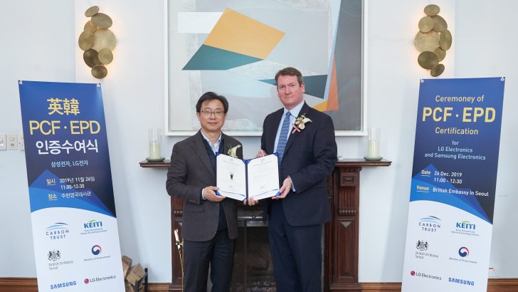
Korea on November 26, 2019
Samsung's 512GB eUFS 3.0 memory to earn Carbon Footprint and Water Footprint Certifications from the globally accredited Carbon Trust
Samsung's 1TB eUFS 2.1 and fifth-generation 512Gb V-NAND also to receive Environmental Product Declaration labels from the Korean Ministry of Environment
Samsung Electronics, a world leader in advanced memory technology, announced that its 512-gigabyte (GB) embedded Universal Flash Storage (eUFS) 3.0 will be awarded Carbon Footprint and Water Footprint Certifications from the highly respected UK-based Carbon Trust during a ceremony at the British Embassy in Seoul, Korea later today. Samsung’s 512GB eUFS 3.0 is the first mobile memory in the industry to be recognized by an international certifying organization, which was made possible through the company’s extensive efforts to reduce carbon and water footprints.
The Carbon Trust is a globally accredited non-profit certification body established by the British government to accelerate the move to a sustainable, low-carbon economy. Each certification by the Carbon Trust was made after a thorough assessment of the environmental impact of carbon emissions and water usage before and throughout the production cycle, based on international standards*.
“We are extremely pleased that our cutting-edge memory technologies not only demonstrate our capability to overcome more challenging process complexities, but also are recognized for their environmental sustainability,” said Chanhoon Park, executive vice president and head of Giheung Hwaseong Pyeongtaek Complex at Samsung Electronics. “Samsung will continue to create memory solutions that provide the highest levels of speed, capacity and power efficiency at extremely small geometries for end-users worldwide.”
Samsung’s Semiconductor Innovations Enable Sustainable Production
Based on the company’s fifth-generation (90+ layers) V-NAND, Samsung’s 512GB eUFS 3.0 provides optimal speed, power efficiency and productivity to deliver twice the capacity and 2.1 times the sequential speed of its fourth generation (64 layers) V-NAND-based 256GB eUFS 2.1, while requiring 30 percent less operating voltage. Additionally, Samsung’s fifth-generation V-NAND utilizes a unique etching technology that pierces more than 90 cell layers in a single precise step. This allows the chip to have nearly 1.5 times more stacked layers than the previous generation and accommodate a 25-percent reduction in chip size. Such innovations help to minimize the overall increase in carbon and water footprints for each V-NAND cell layer.
Samsung is also being awarded Environmental Product Declaration (EPD) labels for its ‘1-terabyte (TB) eUFS 2.1’ and its ‘fifth-generation 512-gigabit (Gb) V-NAND’ by the Korean Ministry of Environment at today’s ceremony.
Samsung plans to actively expand the adoption of its highly sustainable, high-capacity premium memory solutions into many more flagship smartphones and further strengthen global partnerships for its next-generation memory technologies.
*PAS 2050 for carbon footprint and ISO 14046 for water footprint
[Reference] Samsung 512GB eUFS 3.0 environmental footprint (Carbon Trust)
| Carbon Footprint | Water Footprint |
| 13.4 kg CO2 | 0.31 m3 H2O |
*13.4 kg CO2 is comparable to the amount that is absorbed by two 30-year-old pine trees in a year
[Reference] Samsung semiconductor solutions with environmental certifications
| Year | Product | Certification | Accreditation Body |
| 2009 | 64Gb DDR3 (56nm) | Carbon Footprint | Korean Ministry of Environment |
| 2010 | 2Gb DDR3 (46nm) | Carbon Footprint | Korean Ministry of Environment |
| 2010 | 16Gb NAND (42nm) | Carbon Footprint | Korean Ministry of Environment |
| 2012 | 4Gb DDR3 (28nm) | Low Carbon | Korean Ministry of Environment |
| 2012 | 2Gb DDR3 (35nm) | Low Carbon | Korean Ministry of Environment |
| 2012 | 64Gb NAND (27nm) | Low Carbon | Korean Ministry of Environment |
| 2012 | 2Gb LPDDR2 (46nm) | Carbon Footprint | Korean Ministry of Environment |
| 2012 | 4Gb LPDDR2 (35nm) | Carbon Footprint | Korean Ministry of Environment |
| 2012 | 2Gb GDDR5 (35nm) | Carbon Footprint | Korean Ministry of Environment |
| 2012 | 8-megapixel CIS (90nm) | Carbon Footprint | Korean Ministry of Environment |
| 2013 | 4Gb LPDDR3 (35nm) | Carbon Footprint | Korean Ministry of Environment |
| 2013 | Exynos 5410 (28nm) | Carbon Footprint (Industry-first) | Korean Ministry of Environment |
| 2013 | 4Gb GDDR5 (28nm) | Low Carbon (Industry-first) | Korean Ministry of Environment |
| 2013 | 13-megapixel CIS (65nm) | Low Carbon (Industry-first) | Korean Ministry of Environment |
| 2014 | 64Gb NAND (21nm) | Low Carbon | Korean Ministry of Environment |
| 2014 | 4Gb LPDDR3 (25nm) | Low Carbon | Korean Ministry of Environment |
| 2015 | 4Gb DDR4 (25nm) | Carbon Footprint (Industry-first) | Korean Ministry of Environment |
| 2016 | 4Gb LPDDR4 (20nm-class) | Carbon Footprint (Industry-first) | Korean Ministry of Environment |
| 2016 | 64Gb NAND (10nm-class) | Low Carbon | Korean Ministry of Environment |
| 2017 | SSD 850 EVO (250GB) | Environmental Product Declaration (EPD; Industry-first) | Korean Ministry of Environment |
| 2017 | SSD 850 EVO (250GB) | Water Footprint (industry-first) | Korean Ministry of Environment |
| 2017 | 64Gb NAND (10nm-class) | EPD | Korean Ministry of Environment |
| 2018 | SSD 860 EVO (4TB) | EPD | Korean Ministry of Environment |
| 2018 | V4 NAND 512GB | EPD | Korean Ministry of Environment |
| 2018 | 16Gb LPDDR4 | EPD (Industry-first) | Korean Ministry of Environment |
| 2018 | 16Gb LPDDR4X | EPD (Industry-first) | Korean Ministry of Environment |
| 2019 | V5 NAND 512Gb TLC | EPD (Industry-first) | Korean Ministry of Environment |
| 2019 | 1TB eUFS 2.1 | EPD (Industry-first) | Korean Ministry of Environment |
| 2019 | 512GB eUFS 3.0 | Carbon Footprint, Water Footprint (industry-first) |
Carbon Trust |
- 512-gigabyte embedded Universal Flash Storage 3.0
- 512GB eUFS 3.0
- Carbon Trust
- Environmental Product Declaration
- EPD
- Fifth-generation V-NAND
- South Korea Ministry of Environment
- Sustainability
For any issues related to customer service, please go to Customer Support pagefor assistance.
For media inquiries, please click Media Contactto move to the form.