Samsung Mass Produces Industry’s First Application Processor for Wearable Devices Built on 14-Nanometer FinFET Technology
Korea on October 11, 2016

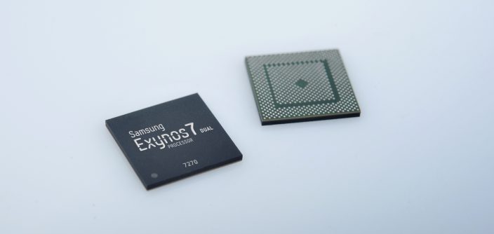
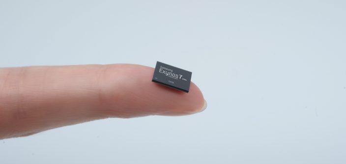
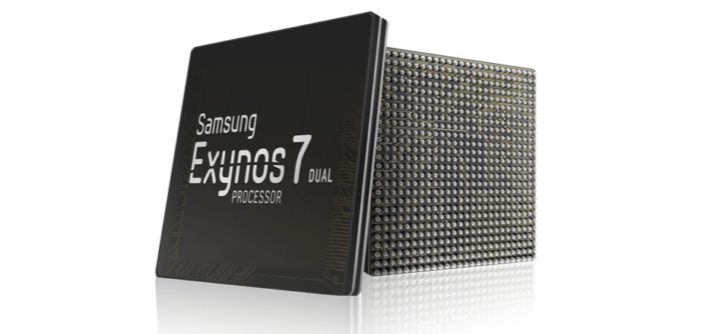
Samsung Electronics, a world leader in advanced semiconductor technology, today announced that it has begun mass production of the Exynos 7 Dual 7270. It is the first mobile application processor (AP) in the industry designed specifically for wearable devices with 14-nanometer (nm) FinFET process technology. It is also the first in its class to feature full connectivity and LTE modem integration.
Since 2015, Samsung has been leading the industry in expanding the adoption of 14nm technology for a wide variety of products from premium smartphones to entry-level mobile devices. With the Exynos 7270, the company also introduces the benefits of this cutting-edge technology to wearables.
“The Exynos 7270 presents a new paradigm for system-on-chips (SoC) dedicated to wearables,” said Ben K. Hur, Vice President of System LSI Marketing at Samsung Electronics. “Designed on our state-of-the-art process technology, this AP offers great power savings, 4G LTE modem and full connectivity solution integration, as well as innovative packaging technology optimized for wearable devices. It is a ground-breaking solution that will greatly accelerate wider adoption of wearable devices by overcoming limitations in current solutions such as energy usage and design flexibility.”
Powered by two Cortex®-A53 cores, the Exynos 7270 makes full use of the 14nm process, delivering 20 percent improvement in power efficiency when compared to its predecessor built on 28nm, and thus notably extending the battery life. By integrating Cat.4 LTE modem, the new AP allows wearables to connect to a cellular service as a stand-alone device. Tethering and data transfer between devices is also possible with its embedded WiFi and Bluetooth connectivity. In addition, integrated connectivity capabilities support FM (frequency modulation) radio, and location-based services with GNSS (global navigation satellite system) solutions.
As well as the implementation of the advanced 14nm FinFET process, Samsung’s innovative packaging technology, SiP(system-in-package)-ePoP(embedded package-on-package), enables the Exynos 7270 to feature outstanding performance and energy-efficiency within a compact solution optimized for wearable devices. The technology combines the AP, DRAM and NAND flash memory chips as well as the PMIC (power management IC) together into a single package. The solution can offer more features than its predecessor in the same 100-square-millimeter (mm2) area while reducing the height by approximately 30 percent. This gives more room for device manufacturers to design high performance, ultra-slim wearable devices.
To expedite the development process, a reference platform comprised of the Exynos 7270, NFC (near field communication) and various sensors is currently available for device manufacturers and customers.
For more information about Samsung’s Exynos products, please visit www.samsung.com/exynos
For any issues related to customer service, please go to Customer Support pagefor assistance.
For media inquiries, please click Media Contactto move to the form.